Jun
15
Pushing Solar to Investment and Efficiency Turning Points
June 15, 2012 | 1 Comment
Two press releases show that both silicon and organic solar are closing in on dramatic cost reductions per watt-hour.
The major market player based on silicon, that’s using about 40% of the overall cost, is getting a new MIT approach that could reduce the thickness of the silicon used by more than 90 percent while still maintaining high efficiency.
The MIT idea is in a pattern of tiny inverted pyramids etched into the surface of the silicon. These tiny indentations, each less than a millionth of a meter across, can trap rays of light as effectively as conventional solid silicon surfaces that are 30 times thicker.
To create the tiny dents, the MIT researchers use two sets of overlapping laser beams to produce exceptionally tiny holes in a layer of material – called a photoresist – that is deposited on top of the silicon. This interference lithography technique is scalable to a large area. Following several intermediate steps, a chemical called potassium hydroxide is used to dissolve away parts of the surface that were not covered by the photoresist. The crystal structure of silicon leads this etching process to produce the desired pyramidal shapes in the surface
The new findings are being reported in the journal Nano Letters in a paper by MIT postdoc Anastassios Mavrokefalos, professor Gang Chen, and three other postdocs and graduate students, all of MIT’s Department of Mechanical Engineering.
The operation of a solar cell occurs in two basic steps: First, an incoming particle of light, called a photon, enters and is absorbed by the material, rather than reflecting off its surface or passing right through. Second, electrons knocked loose from their atoms when that photon is absorbed then need to make their way to a wire where they can be directed out to produce an electrical current, rather than just being trapped by other atoms.
The problem – most efforts to increase the ability of thin crystalline silicon to trap photons – such as by creating a forest of tiny silicon nanowires on the surface – also greatly increase the material’s surface area, increasing the chance that electrons will recombine on the surface before they can be harnessed.
MIT’s new approach avoids that problem. The tiny surface indentations – the team calls them “inverted nanopyramids” – greatly increase light absorption, but with only a 70 percent increase in surface area, limiting surface recombination. Using this method, a sheet of crystalline silicon just 10 micrometers (millionths of a meter) thick can absorb light as efficiently as a conventional silicon wafer 30 times as thick.
The solar panel package as a whole is simply lighter, cut the weight of the cells, which in turn would reduce the material needed for frames and supports.
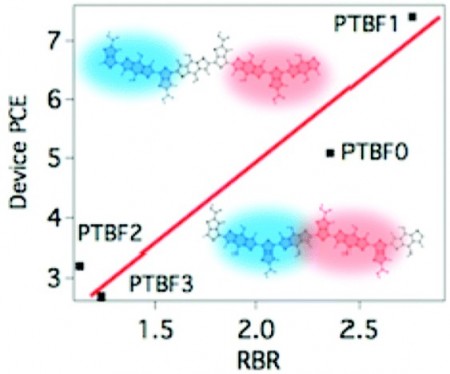
On the organic front the Argonne National Laboratory’s senior chemist Lin Chen and her colleagues examined how four different molecules in the polymer layer in the middle of a solar cell generated different exciton dynamics. They discovered that more heavily polarized excitons yielded more efficient polymer-based solar cells.
Chen explains, “The real question that this work tries to answer is how to design a material that will make splitting the exciton require less energy. The closer the hole and the electron regions are inside an exciton, the more likely they are to recombine without generating electricity. But if they are already ‘pre-separated,’ or polarized, the more likely they are to escape from this potential trap and become effective charge carriers.”
There’s that ‘recombine’ problem again. There’s a strong natural attraction between the positive and negative charges that a photon generates after it strikes the cell, but in order to capture the energy, these charges need to be kept separate.
When these charges are still bound together, they are known to scientists as an exciton. Excitons can be thought of as a sort of “quasiparticle,” Chen explained, because they exhibit certain unique behaviors. When the two charged regions of the exciton – the electron and a region known as a “hole” – are close together, they are difficult to pry apart.
When energy is added to the system, however, the charges begin to separate, rendering the electrons and holes completely free and eventually allowing for the possibility of generating current and extracting electricity.
Chen explains, “If the conventional exciton, right after it is generated, contains the hole and electron in almost the same location, these new materials are generating an exciton that is much more polarized at the beginning.” Currently, the collaborative team is exploring new materials for high-efficiency organic solar cells based on these findings.
So far the organic solar cells still have a wide gap to match the efficiency of their inorganic, silicon-based competitors, but they remain much more attractive from a cost perspective.
Chen’s work has been published in the Journal of the American Chemical Society.
At the moment silicon has a big efficiency advantage per exposed area and organics have a huge cost advantage. Worldwide the installation of solar panels is growing at breakneck pace. Where the grid is weak or missing solar is a huge boon to development.
In the developed economies solar is at a major competitive disadvantage. Still, the allure of free energy with a massive investment attracts romantics, early adopters and government subsidies. Grousing included, the world market benefits from taxpayer largess. Eventually the research and scale of production will “trickle back up” to the developed economies.
Solar is an energy source that can’t be denied, it will only get better.
Comments
1 Comment so far


This technology basically already exists, and is being commercialized by a joint effort between Natcore Technologies, and the NREL.