Oct
2
A New Synthesized Perovskite Solar Cell Developed
October 2, 2018 | Leave a Comment

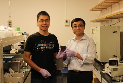
Dr. Zonghao Liu (left) and Prof. Yabing Qi (right) with the 5 cm × 5 cm perovskite solar module that they developed in their lab at OIST. Image Credit: Okinawa Institute of Science and Technology Graduate University. Click image for the largest view.
Professor Yabing Qi and his team from OIST in collaboration with Professor Shengzhong Liu from Shaanxi Normal University, China, developed the cells using the materials and compounds that mimic the crystalline structure of the naturally occurring mineral perovskite.
The team described their technique in a study published in the journal Nature Communications.
In what Professor Qi refers to as “the golden triangle,” solar cell technologies need to fulfill three conditions to be worth commercializing: their conversion rate of sunlight into electricity must be high, they must be inexpensive to produce, and they must have a long lifespan. Today, most commercial solar cells are made from crystalline silicon, which has a relatively high efficiency of around 22%. Though silicon, the raw material for these solar cells, is abundant, processing it tends to be complex and shoots up the manufacturing costs, making the finished product expensive.
Perovskite offers a more affordable solution, Professor Qi said. Perovskite was first used to make solar cells in 2009 by Prof. Tsutomu Miyasaka’s research team at Toin University of Yokohama, Japan, and since then it has been rapidly gaining importance.
“Research on perovskite cells is very promising. In only nine years, the efficiency of these cells went from 3.8 % to 23.3%. Other technologies have taken over 30 years of research to reach the same level,” explained Qi. The fabrication method he and his research team have developed produces perovskite solar cells with an efficiency comparable to crystalline silicon cells, but it is potentially much cheaper than making silicon solar cells.
To make the new cells, the researchers coated transparent conductive substrates with perovskite films that absorb sunlight very efficiently. They used a gas-solid reaction based technique in which the substrate is first coated with a layer of hydrogen lead triiodide incorporated with a small amount of chlorine ions and methylamine gas – allowing them to reproducibly make large uniform panels, each consisting of multiple solar cells.
In developing the method, the scientists realized that making the perovskite layer 1 micron thick increased the working life of the solar cell significantly. “The solar cells are almost unchanged after working for 800 hours,” says Dr. Zonghao Liu, a postdoctoral scholar in Prof. Qi’s research unit at OIST and the first author of the study.
In addition, a thicker coating not only boosted the stability of the solar cells but also facilitated the fabrication processes, thereby lowering its production costs. “The thicker absorber layer ensures good reproducibility of solar cell fabrication, which is a key advantage for mass manufacturing in the realistic industrial-scale setting,” said Dr. Liu.
The big challenge Professor Qi and his team now face is in increasing the size of their newly designed solar cell from the 0.1 mm square sized prototype to large commercial-sized panels that can be several feet long. This is where the industry can help.
“There exists a large gap between the findings in lab and reality, and the industry is not always ready to cover this entire gap by itself. So, the researchers need to take one more necessary step beyond their labs and meet the industry half-way,” said Qi.
To take that step, Prof. Qi and team received a generous grant from OIST’s Technology Development and Innovation Center, under their Proof-of-Concept Program. With that funding, the team has built a working model of their new perovskite solar modules consisting of multiple solar cells on 5cm × 5cm substrates, with an active area of 12 square cm – much bigger than their experimental prototype but smaller than what is required for commercial purposes.
Although the process of up-scaling has reduced the efficiency of the cells from 20% to 15%, the researchers are optimistic that they will be able to improve the way they work in the coming years and successfully commercialize their use.
This pretty encouraging work. 20 percent efficiency at low cost is enticing, while 15% not so much. Where that 25% loss is caused must be of some considerable interest.
The new fabrication process looks very promising, as the scale loss is sure to be found and more efficiency is likely in there to be developed. With fresh funding this technology will likely pay off for producers and consumers. We’ll probably not be told in a few years our new device has this technology, but the device will cost less.

