Mar
12
A Lot of Good LED and Solar Cell News
March 12, 2014 | Leave a Comment
Three research papers with LED and/or for solar cell progress all published in the past few days. The three are based on one material. MIT, TU Vienna, and University of Washington (UW) researchers have all made recent advances on PV cells, LEDs, and other optoelectronic components made possible using an ultrathin tungsten diselenide film.
There is also another material hot off the press too. We’ll get to that in a bit.
The TU Vienna paper that got the press release out first shows experiments of the material may be used to create ultrathin flexible solar cells. Even flexible displays could become possible.
The UW scientists have built the thinnest known LED that can be used as a source of light energy in electronics. The UW LED is based off of two-dimensional, flexible semiconductors, making it possible to stack or use them in much smaller and more diverse applications than current technology allows.

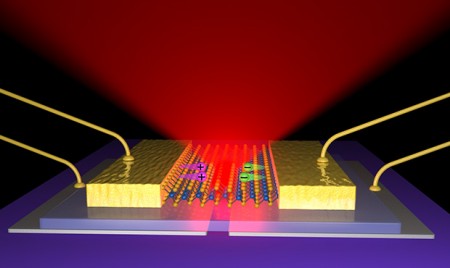
A graphical representation shows the layers of the 2-D LED and how it emits light. Click image for the largest view. Image Credit: University of Washington.
A team of MIT researchers has used this novel material that’s just a few atoms thick to create devices that can harness or emit light.

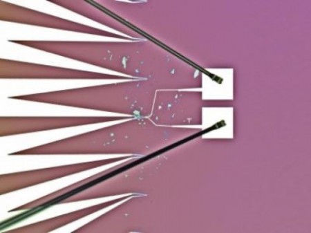
The MIT team’s experimental setup where electricity was supplied to a tiny piece of tungsten selenide (small rectangle at center) through two gold wires (from top left and right), causing it to emit light (bright area at center), demonstrating its potential as an LED material. Click image for the largest view. Image Credit: Britt Baugher and Hugh Churchill at MIT.
LEDs are diodes, a kind of electron one way valve, that are usually made by “doping” a process of injecting other atoms into the crystal structure of a host material. From that its possible to make either of the two basic kinds of semiconducting materials, p-type or n-type.
What tungsten diselenide offers is either p-type or n-type functions can be obtained just by bringing the vanishingly thin film into very close proximity with an adjacent metal electrode, and tuning the voltage in the electrode from positive to negative. That means the material can easily and instantly be switched from one type to the other, which is rarely the case with conventional semiconductors.
UW’s LED has been recently identified as the thinnest-known semiconductor. The researchers use regular adhesive tape to extract a single sheet of the material from thick, layered pieces in a method inspired by the 2010 Nobel Prize in Physics awarded to the University of Manchester for isolating one-atom-thick flakes of carbon, called graphene, from a piece of graphite.
The MIT team produced a device with a sheet of WSe2 material that was electrically doped half n-type and half p-type, creating a working diode that has properties very close to the ideal.
The TU Vienna tungsten diselenide consists of one layer of tungsten atoms, which are connected by selenium atoms above and below the tungsten plane. The material absorbs light, much like graphene, but in tungsten diselenide, this light can be used to create electrical power.
Now for the second material. A Fraunhofer-Gesellschaft team has found a way to make LED lamps even more compact while supplying more light than commercially available models. The key to their success is transistors made of the semiconductor material gallium nitride.

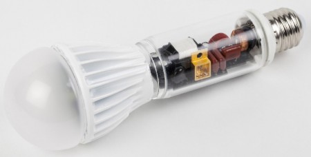
Gallium Nitride Tranistors in a Flashlight. Click image for the largest view. Image Credit: Fraunhofer Institute for Applied Solid State Physics IAF.
LEDs are not a perfect answer. They are extremely sensitive to variations and spikes in power. To function properly, they need a driver that ensures a constant supply of power at all times. This driver, which takes the alternating current from the grid and converts it into direct current with a reduced voltage, has a profound influence on the light yield and lifetime of the LED lamp as a whole.
Naturally the driver is an added cost in building a bulb and the demands placed on the driver electronics are correspondingly high. This is where the Fraunhofer Institute work has an advantage near term. During practical testing, the scientists found that the drivers developed using this new semiconductor material were extremely robust. Components made of GaN can operate at higher currents, voltages and temperatures than standard silicon transistors.
Dr. Michael Kunzer, group manager at Fraunhofer explains gallium nitride transistors can also switch at high frequencies. The switching speed has a significant impact on the size of the coils and condensers built into the drivers for energy storage. In a GaN-based driver, the switch speed can be made as much as a factor of 10 faster than that of its silicon equivalent. “Applied to a smaller surface, this means it is possible to make switching cheaper. The whole LED lamp can be made lighter and more compact while delivering the same or even improved illumination.”
The Fraunhofer scientists were able to increase the light output. While the luminous flux of commercial LED retrofit lamps featuring silicon components is around 1000 lumen (the unit used to measure the light produced), the researchers have been successful in increasing this to 2090 lumen.
MIT’s Pablo Jarillo-Herrero, the Mitsui Career Development Associate Professor of Physics overviews the tungsten diselenide research with, “Because this material can be engineered to produce different values of a key property called bandgap, it should be possible to make LEDs that produce any color — something that is difficult to do with conventional materials. And because the material is so thin, transparent, and lightweight, devices such as solar cells or displays could potentially be built into building or vehicle windows, or even incorporated into clothing.”
UW’s Xiaodong Xu, assistant professor in materials science and engineering and in physics points out, the technology could open doors for using light as interconnects to run nano-scale computer chips instead of standard devices that operate off the movement of electrons, or electricity. The latter process creates a lot of heat and wastes power, whereas sending light through a chip to achieve the same purpose would be highly efficient. “A promising solution is to replace the electrical interconnect with optical ones, which will maintain the high bandwidth but consume less energy. Our work makes it possible to make highly integrated and energy-efficient devices in areas such as lighting, optical communication and nano lasers,” Xu said.
It looks like a new field is opening up for LEDs and perhaps in time solar cells and displays. One might expect with this much improvement that manufactures are watching closely.
LEDs are going to get more efficient, run cooler and cost less. Even today’s products are plunging in price. Lets hope the new technologies can accelerate that pace.


